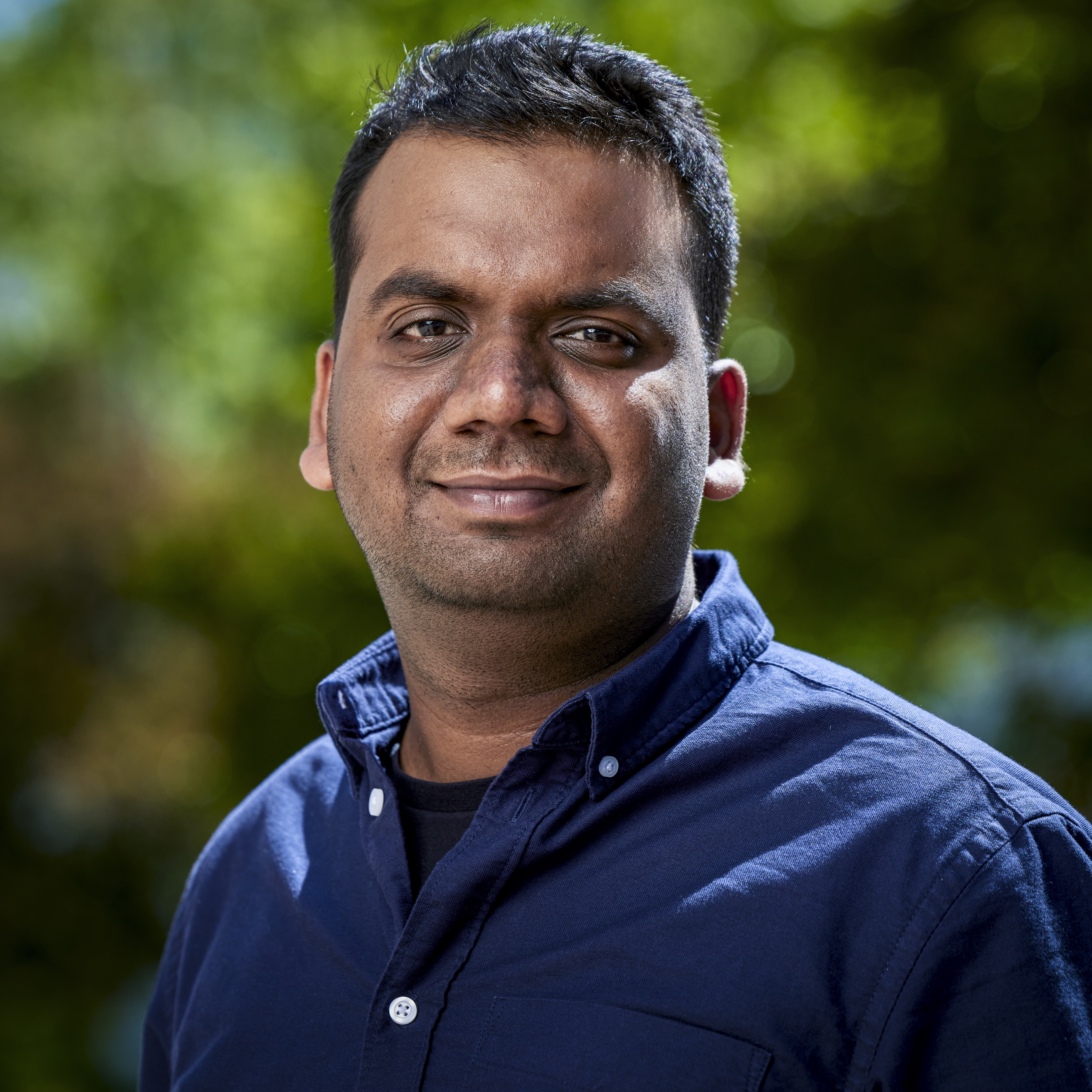
About me
I am currently working as a Process Engineer in the ALD deposition product group at Lam Research. Prior to Lam, I completed my Ph.D. in Chemical Engineering at UC Berkeley and my B.S. and M.S. in Chemical Engineering at IIT Delhi, India. At Lam, I have developed a new low dielectric constant ALD liner for future Through-Silicon Via (TSV) nodes, evaluated hardware components to improve the throughput of Lam’s Striker chambers, and screened multiple ALD precursors for carbon- and fluorine-doped silicon oxide and nitride films. For these projects, I coordinated and drove a multinational team of software, mechanical, electrical, and RF plasma engineers, together with Lam’s Field Service Engineers in Taiwan, to ensure smooth project execution. Taken together, these experiences spanning semiconductor product development, advanced materials research, energy technologies, and mathematical modeling have given me a strong technical foundation and a broad cross-industry perspective on how technologies evolve from concept to implementation.
At Lam, I am the point of contact for Lam’s engagement with Taiwan-based world’s largest chip manufacturer, where numerous Striker Oxide Chambers are in production. Together with our customers, I have worked on evaluating multiple hardware changes to increase throughput, which has given me a deep insight into the workings of ALD chambers. Currently, I am also evaluating a new RF generator system for next-generation ALD chambers at Lam. One of my biggest achievements at Lam is the development of a new low-k dielectric liner for TSV holes in advanced packaging applications. Since this lower dielectric constant is achieved by doping silicon oxide with foreign elements, the development process has given me expertise in thin-film metrology, including Ellipsometry, FTIR, SIMS, XRR, XPS, STEM, XSEM, and CV/IV. Additionally, I am also responsible for successfully demonstrating the first diffusion-barrier PECVD silicon nitride film in Lam’s Striker Chambers and solving the crucial problem of defects arising from interfaces between oxide and nitride films. Integrating these new materials and processes into the existing manufacturing workflow also gave me the opportunity to learn crucial fundamentals associated with process integration.
For my doctoral dissertation, I developed a new statistical-physics–based theory to model electrical double layers in concentrated electrolyte solutions, gaining expertise in chemical physics, materials science, and computational physics. This expertise in electrical double layers, being directly relevant to plasma processes, led me to accept a Process Engineer position in the PEALD product group at Lam Research. During my Ph.D., I also did internships in machine learning for materials science, Monte Carlo methods, molecular dynamics, and data science. I also worked extensively on experimental photocatalyst development and characterization during my undergraduate years. Overall, I believe I bring the perfect combination of experimental, theoretical, and computational experience that positions me ideally to contribute to new process development, integration, and hardware engineering. Being an experimentalist who also understands physical modeling, I can collaborate with mechanical engineers on new product development and evaluation. My computational experience further provides a solid foundation in data management, analysis, and equipment intelligence, which are increasingly important in process engineering.